Overview
Product Details
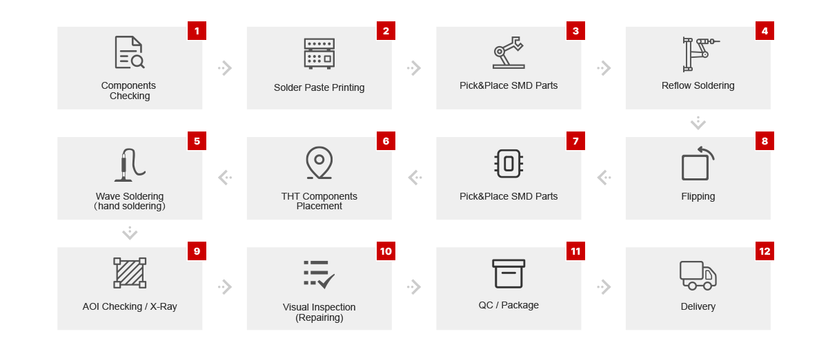
PCB Assembly Process

NextPCB provides efficient and high-quality turnkey PCB assembly service to its customers. In order to achieve the fastest possible turnaround of the highest quality product, we continuously strive to improve our services and to make each step as efficient as possible. One of the most important factors in the overall efficiency of each PCB assembly project is the client’s understanding of PCB assembly process.
This page provides an overview of some standard but important turnkey PCB assembly process. This is a brief overview only, if you are more interested in, welcome to our factory.Incoming Material Inspection
An incoming inspection, also known as a receiving inspection or material inspection, validates the quality of purchased raw materials based on set acceptance criteria. It is performed by quality assurance personnel in the manufacturing facility to resolve quality issues during pre-production. Incoming inspection results follow an identification tagging system to determine required actions when an item is tagged as accepted, conditionally accepted, or rejected.
NextPCB team will do full check on incoming material inspection to control the assembly quality. Components counting, package confirm, quantity confirm are in this process.
SMT Solder Paste Printing
Solder paste (or solder cream) is a material used in the manufacture of printed circuit boards to connect surface mount components to pads on the board. Before soldering, all PCB boards should print solder paste so that the components can be soldered by pick & place machine.
Pick & Place Assembly
Once bare PCBs printed solder paste, they are moved to NextPCB’s automated Pick & Place machines for the actual mounting of components on their associated pads. Part placement is 100% machine automated for maximum accuracy and efficiency, and uses the project’s Centroid file for component coordinates and rotation data. The boards are again inspected after components have been mounted to ensure all placements are accurate before the soldering process begins.
Reflow Soldering
With parts mounted securely in place with solder paste underneath their pads, it is time for the PCBs to enter the reflow soldering oven. This is the most common method for PCB assembly in the industry today since it is much more flexible in terms of PCB layout requirements compared with wave or hand soldering. Most of the time, NextPCB can use reflow soldering for a majority of the parts on a board, and then pass the mostly-assembled boards to our highly skilled hand soldering team for the final few connectors and through hole components. NextPCB has more than 6 reflow oven in its plant.
Wave Soldering
Wave soldering is a large-scale soldering process by which electronic components are soldered to a printed circuit board (PCB) to form an electronic assembly. The name is derived from the use of waves of molten solder to attach metal components to the PCB. It is for Through hole components soldering. Normally if your order is small, it will not be soldered by wave soldering machine. If you insist, extra fee will be added.
NextPCB.net is a shenzhen PCB assembly manufacturer famous for its China turnkey PCB assembly. Our PCB assembly house is located in Shenzhen, China, with multiple wave soldering machines. If you're interested in PCB assembly quote, or if you're wondering about the PCB assembly cost, please contact us and we'd love to answer your questions. We support low volume PCB assembly, light PCB assembly and prototype assembly.

